Lithographic Material Innovation Continues to Enable the Semiconductor Industry
January 19, 2026
As artificial intelligence (AI), high-performance computing (HPC), 5G, and big data continue to grow exponentially, the demand for advanced memory and logic chips is rising in parallel. Lithography, the essential process in semiconductor fabrication that enables ultra-precise patterns on silicon wafers using advanced materials and cutting-edge technologies, sits at the center of this progress. It is a key driver of node scaling and more sustainable manufacturing. But meeting these requirements depends on continuous innovation in materials.
Established as an independent company in November 2025, Qnity brings decades of expertise to advanced lithography materials innovation (see Figure 1). In fact, our team introduced the first commercial i-line photoresist in 1987. And 20 years ago, we invented embedded barrier layer technology for 193 nm immersion lithography, generating a protective barrier during photoresist coating. In 2025, the American Chemical Society recognized Qnity scientists as Heroes of Chemistry for developing embedded barrier layer technology, which improved yield, reduced defectivity, increased efficiency, and simplified early immersion processes. Photoresists with embedded barrier layer technology remain widely used, a testament to how Qnity’s materials expertise continues to push the industry forward.
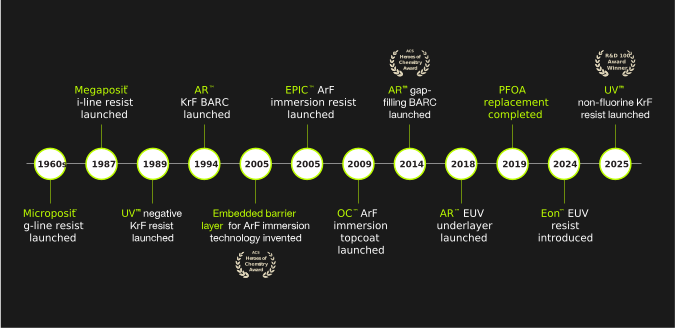
Figure 1. Qnity has consistently developed breakthrough material innovations with each new generation of lithographic technology.
This pioneering spirit perfectly positions Qnity to address today’s most pressing lithography challenges using novel polymer and organic chemistry, exploring new techniques, and collaborating closely with our customers and partners.
Challenges for advanced chip manufacturing
As lithographic patterning pushes into advanced nodes for AI, HPC, 5G, and data-centric applications, chipmaking requires more complex lithography techniques in order to achieve optimal resolution and yield. Today, advanced circuit manufacturing faces three key challenges, each of which creates corresponding issues for lithography:
- Scaling down of critical dimensions (CD)
- Growing prevalence of 3D structures
- The need for more sustainable manufacturing
Let’s take a closer look at each of these problems, their evolutionary paths, and some of the material solutions Qnity offers to address them. For each challenge, material solutions have been devised at both the photoresist level and at the functional layer, i.e., below and above the photoresist.
CD Scaling
Photoresist chemistry is primarily a function of wavelength. The challenge of tuning photoresists for wavelength reduction has driven lithography scaling for more than 50 years. When scaling demands moved the needle down to 248nm in the late 1980s, faster and more transparent resists were needed. Copolymers based on p-hydroxystyrene and t-butyl acrylate were especially successful and became the standard-bearers for high-volume IC production.
Ten years later, the industry again scaled down, to the 193nm wavelength, requiring resist chemists to start once more from scratch to meet new transparency and etch-resistance constraints. Once the proper resin systems were identified, chemical amplification was applied to meet throughput requirements, and 193nm resists continued to evolve as imaging transitioned from dry to immersion lithography. Extending 193nm immersion lithography has allowed patterning far below the exposing wavelength.
Today, supporting AI, HPC, and other advanced applications means pushing into sub-2 nm nodes and increasingly relying on extreme ultraviolet (EUV) lithography and soon, high-NA EUV. This shift introduces new challenges for CD scaling, including:
- Poor resist resolution
- Poor line width roughness (LWR)/CD uniformity of resist
- Reduced process window
- Slow photo speed
At the resist level, materials are needed that offer compatibility with shorter wavelengths, high resolution, good LWR and profile, wide process window, and fast photo speed. Qnity has developed solutions that tackle these requirements.
Functional layer material solutions for below and above the resist include:
- Antireflective coating materials (BARCs) and EUV interlayers deliver low reflectivity, a wide process window, and fast etching properties, while gap-fill materials provide good gap-filling and planarization performance, along with superior wet etching resistance
- Advanced overcoats enable line CD shrink, and improve line edge roughness after normal lithography process. Qnity’s CTO™ chemical trim overcoat is a photoresist-trimming solution used to form finer and smoother photoresist patterns than those with direct imaging alone. A chemical trim process typically involves coating a chemical trimming overcoat over a photoresist pattern, heating the wafer so that acid diffuses into the photoresist pattern and causes deprotection in a resist surface region, and developing the pattern to remove the surface region, thereby achieving smaller CD and smoother pattern.
- Qnity’s next-generation EUV portfolio strengthens this ecosystem. The Eon™ EUV resist platform is designed for higher resolution, improved LWR, strong CD uniformity, and faster photo speed to meet the demands of EUV and high-NA EUV. Paired with AR™ EUV underlayer, which enhances photospeed and improves process window and pattern fidelity, these materials work together to support advanced semiconductor manufacturing at sub-7nm nodes.
3D Topography
As device architectures continue to scale, 3D structures are now playing a key role in boosting density, improving power efficiency, and delivering the performance needed for AI and HPC. What started with the move from planar transistors to fin field-effect transistors (FinFETs) has grown into a much larger shift toward vertical integration across the industry. 3D NAND now relies on hundreds of stacked layers and is rapidly moving toward 500 or more.1 DRAM is evolving through silica via (TSV)-based stacking in high-bandwidth memory (HBM), and logic is transitioning from FinFET to gate-all-around (GAA) beginning at the 3 nm node2, supported by backside power delivery and advanced 3D packaging approaches such as chiplets and hybrid bonding.
These increasingly complex 3D topographies introduce significant challenges for lithography. Patterning over deep structures requires materials that can handle height variations, minimize reflectivity, maintain profile control, and fill high-aspect-ratio gaps without voids. To address these needs, novel BARC and gap-fill materials are needed that offer fast dry etching properties but good wet etching resistance, good planarization, and, in particular, the ability to fill gaps caused by 3D topography without creating voids.
Qnity’s suite of application-specific BARCs and gap-fill materials meets these requirements, helping the industry address patterning challenges associated with scaling and 3D structures. At the resist level, Qnity solutions that are helping chipmakers cope with 3D topography challenges include:
- UV™ thick negative-tone KrF/248 nm resists for 3D NAND
- Epic™ 193 nm resists that provide excellent CD uniformity, LWR, and profile control
- Gap-fill materials with strong wet etch resistance to support evolving logic architectures
- Eon™ positive-tone resists for EUV lithography that improve resolution, line edge roughness and sensitivity
These materials, together with reflection-control layers such as BARC and topcoat, and innovations like embedded barrier layer technology that can simplify production processes, are valuable components for next-generation 3D integration.
Sustainability
There’s no getting around the fact that chip fabrication has become both more complex and resource-intensive. Sustainability is quickly moving from a box that’s nice to check off to a core requirement for advanced semiconductor fabricators. Globally, companies across the semiconductor supply chain are facing stronger ESG expectations and tightening per- and polyfluoroalkyl substances (PFAS) regulations. Advocacy is underway to build understanding for essential use in chip manufacturing and the critical role of semiconductors to the global economy3, yet the overall direction is clear. The industry is seeking safer and more sustainable material options.
Qnity’s approach focuses on developing advanced materials that meet stringent performance requirements for leading-edge nodes while supporting sustainability goals for customers, such as eliminating substances of concern, enhancing safety, and ensuring long-term reliability. A major focus is advancing non-fluorine technologies in lithography materials, and our team’s progress is already being recognized. UV™ 26GNF photoresist, a commercially available KrF resist that substitutes industry-standard PFAS-containing compounds with non-fluorine alternatives was recognized with the R&D 100 Award. This material delivers the control and consistency required for high-volume manufacturing. UV™ 26GNF represents a real, commercially available step forward in sustainable lithography materials. Building on this success, Qnity is expanding our non-fluorine lithography materials family across other wavelengths and nodes, reinforcing its leadership in semiconductor innovation.
And no matter the innovative material we develop, collaboration plays a significant role. We work closely with chipmakers to match new material platforms with customer sustainability goals. This might mean reducing hazardous substances, improving process efficiency, or lowering overall resource use. Together, we are all helping move the semiconductor industry toward a more sustainable future.
As this overview has illustrated, Qnity is well established as an industry leader in electronic and lithographic materials. Innovations like BARC, gap-fill materials, and advanced photoresists have addressed critical challenges in CD control, planarization, etch selectivity, and the growing complexity of 3D device structures. As we look ahead to what’s next, lithography will remain key to the semiconductor industry’s explosive growth, which SEMI projects will surpass $1 trillion by 2030.4 New challenges will emerge, sustainability will become even more critical, and advanced materials will continue to shape what is possible in lithography. Through it all, Qnity will remain a trusted partner in delivering the solutions that move the industry forward.
Sources:
1 Semiconductor Engineering, 2024.
2 Semiconductor Engineering, 2020.
3 Semiconductor Industry Association, 2023.
4 Electronics Weekly, 2025.
Related Information
Qnity develops and delivers market-leading lithography materials to support semiconductor advanced patterning.
Qnity offers complete line of anti-reflectant coatings and functional sublayer products include bottom anti-reflective coatings (BARCs), spin-on-carbons (SOCs) and extreme ultraviolet (EUV) underlayers.
Qnity offers robust, production-proven photoresists for lithography that meet the requirements of generations of semiconductor processes.
We’re here to help.
We love to talk about how our electronics solutions can build business, commercialize products,
and solve the challenges of our time.