Powering AI at Scale with Embedded Capacitance Materials
June 29, 2026
As AI, cloud computing, and data centers continue to scale, so do their power demands—and the complexity of the systems that support them. These next-generation architectures rely not only on advanced chips, but also on high-performance connectivity and advanced interconnect solutions that enable fast, reliable data flow across increasingly dense designs.
Today’s high-performance processors operate at lower voltages but draw significantly higher currents—creating new challenges for power delivery networks (PDNs). Ensuring stable power while maintaining signal integrity across advanced interconnect architectures is no longer just a design requirement—it’s a critical enabler of system performance, reliability, and scalability.
In this blog, we explore how embedded capacitor materials—especially ultra-thin laminates—are redefining PDN performance for next-generation electronics.
Why PDNs are under pressure
Modern AI processors and ASICs (Application-Specific Integrated Circuits) can draw thousands of amps of current, often switching at extremely high speeds. These fast current changes can introduce:
- Voltage ripple
- Power noise
- Signal integrity issues
- Electromagnetic interference (EMI)
Traditionally, designers rely on surface-mounted capacitors and voltage regulators to manage these effects. However, these approaches are reaching their limits as systems become more compact and demanding. These challenges are amplified in systems with advanced interconnect densities and high-speed connectivity requirements, where power integrity and signal integrity must work together.
Embedded capacitors: a smarter approach
Embedded capacitors integrate capacitance directly inside the PCB stack-up, rather than placing components on the board surface.
This approach delivers two major advantages:
- Reduced inductance
By placing capacitance closer to the IC, current paths become shorter. This significantly reduces loop inductance, which is often the primary cause of power noise. - Improved high-frequency performance
Embedded capacitance provides a low-inductance path for high-frequency currents, improving decoupling effectiveness where traditional capacitors struggle.
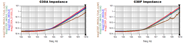
The role of ultra-thin laminates
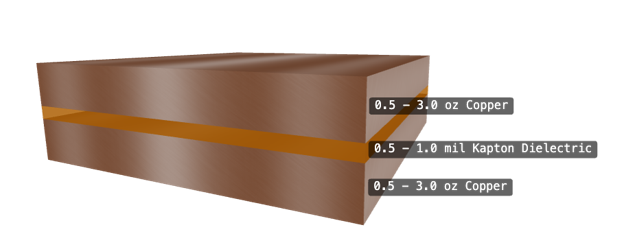
One of the most effective ways to implement embedded capacitance is through ultra-thin dielectric laminates, such as Interra® HK04J.
These materials consist of thin dielectric layers sandwiched between copper planes, forming a distributed capacitance structure within the PCB.
Key features:
- Thickness as low as 12 µm–25 µm
- Compatible with standard PCB processes
- Stable performance across frequency and temperature
- Supports high-speed, high-current designs
What really drives performance?
It’s tempting to assume that more capacitance = better performance. However, the study shows something more important:
Reducing inductance is the real game changer.
While embedded materials do increase capacitance, the biggest benefit comes from dramatically lowering loop inductance, which:
- Improves power delivery efficiency
- Expands the effective bandwidth of decoupling capacitors
- Reduces voltage ripple during fast switching
Measurable improvements in real systems
Lower loop inductance
Using ultra-thin embedded capacitance layers can reduce loop inductance by up to 80–90% when optimally placed.
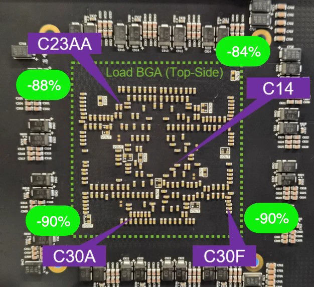
Picture of Capacitor Locations for load board
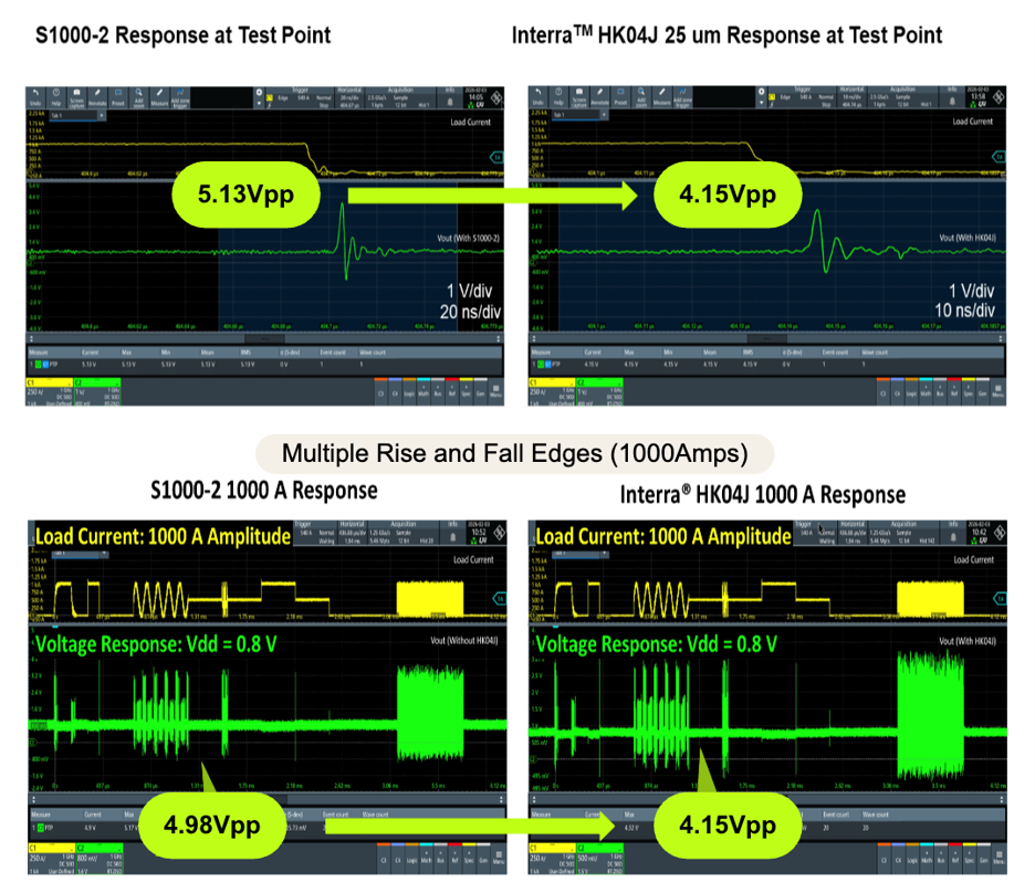
Better transient response
When tested under high current load conditions:
- Voltage fluctuations were reduced by up to 40%
- Power rail stability improved significantly
- Ringing and noise were minimized
Reduced noise and EMI
Embedded capacitance also helps:
- Spread current more evenly across the board
- Lower peak current densities
- Reduce conducted and radiated EMI
This is especially critical in dense AI and data center hardware.
Why placement matters
Not all PCB stack-ups deliver the same benefit.
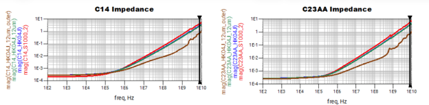
The research shows that the best performance comes from placing ultra-thin embedded capacitance layers on the outer power/ground planes.
This configuration:
- Minimizes loop inductance most effectively
- Improves transient response
- Provides the flattest impedance profile across frequencies
Additional design benefits
- Fewer discrete components
In lower-power designs, embedded capacitance can reduce the number of surface capacitors—saving space and simplifying BOMs. - Improved thermal performance
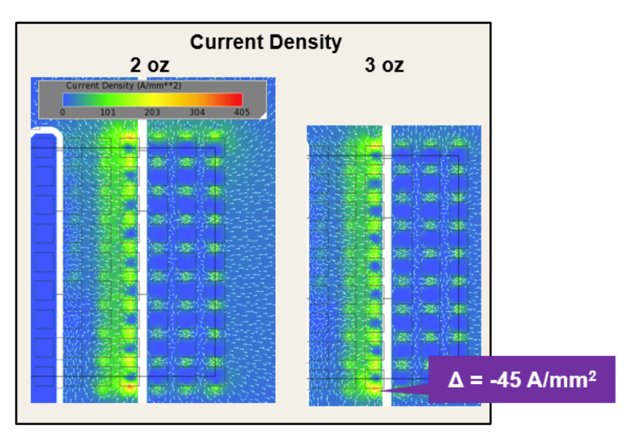
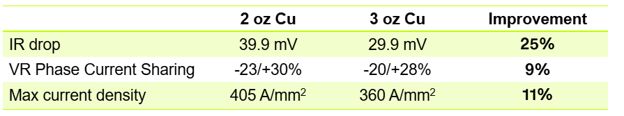
When combined with thicker copper layers:
- IR drop can improve by ~25%
- Current distribution becomes more efficient
- Heat generation is reduced
What this means for AI and data centers
As systems continue to scale, embedded capacitor materials are becoming an essential tool for:
- High-current ASICs
- GPUs and AI accelerators
- Networking and cloud infrastructure
They enable designers to push performance limits without sacrificing stability or reliability.
Key takeaways
- Embedded capacitors improve PDN performance by reducing inductance—not just adding capacitance
- Ultra-thin laminates enable faster, cleaner power delivery
- Proper stack-up design is critical to maximizing benefits
- The result is lower noise, improved efficiency, and more reliable high-performance systems
Looking ahead
As AI workloads grow and power demands increase, innovations like embedded capacitance will play an even larger role in enabling next-generation hardware.
By integrating power integrity directly into the PCB structure, designers can build systems that are not only faster—but also more stable and efficient.
Acknowledgment
This work was made possible through close collaboration and technical contributions from industry leaders in signal integrity, measurement, and power integrity solutions.
We would like to sincerely thank:
- Signal Edge Solutions for their expertise in system-level modeling and power integrity analysis
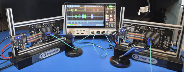
- Picotest for their design, advanced measurement tools and validation support
- GCE (Gold Circuit Electronics) for their contributions to test platform development and execution
Their partnership was instrumental in validating the performance of embedded capacitor materials and advancing this study.
We’re here to help.
We love to talk about how our electronics solutions can build business, commercialize products,
and solve the challenges of our time.